Overview | Standard Features | Available Options | Specifications | Controlled | Atmosphere Furnace | Flux Coaters | Wafer Handlers |
| |
|
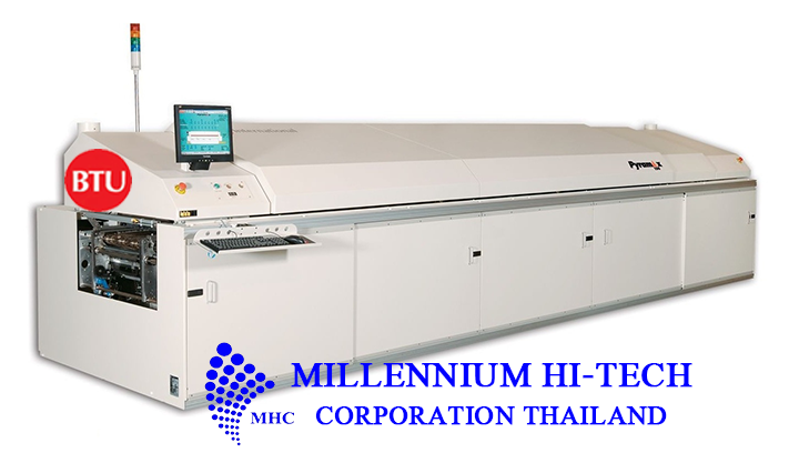
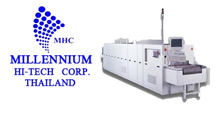
Overview
Take your wafer bump reflow process to the next level.
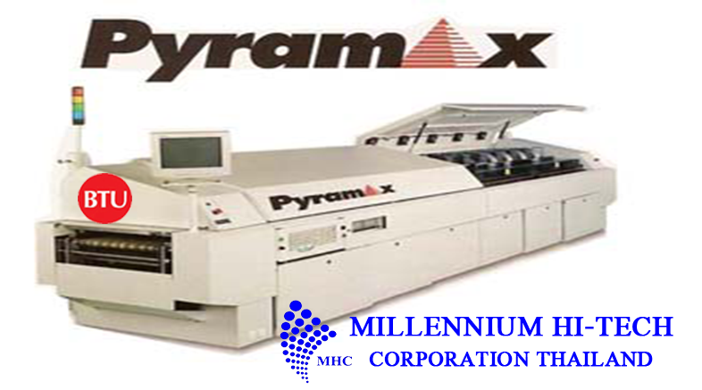
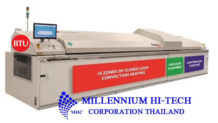
Quality, consistency and control. That’s what you can expect from the BTU Controlled Atmosphere Furnace. Specifically designed to meet wafer-level packaging demands, the TCAS is configured to meet exact process requirements. Available for nitrogen or hydrogen processing or a mixture of both, the TCAS delivers excellent atmosphere purity, high throughput and flux-free continuous processing. The end result is superior efficiency, superior performance, and superior thermal uniformity. So take advantage of the TCAS – and take your wafer bump reflow process to the next level. |
|
|
STANDARD FEATURES INCLUDE:
Flexible Configurations
Zone lengths and gas barrier positions can be optimized for precise control over one thermal profile or maximum flexibility for multiple profiles.
600oC Maximum Temperature
Provides the most flexibility for processing eutectic, lead-free, and high lead solders all in one system.
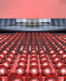
Standard Packaging Configuraton
Achieves O2 levels down to 2ppm, reducing the likelihood of bad solder joints by preventing oxidation. |
AVAILABLE OPTIONS INCLUDE:
Automated Wafer Handler Option
200mm and 300mm handling options allow full process automation and yield improvement by preventing contamination and wafer breakage.
Hydrogen Atmospheres up to 95%
System interlocks and a fail-safe gas panel ensure reliable H2 processing for oxide-free solder reflow, eliminating flux and cleaning of bumped wafers.
SEMI S2/S8 Compliance
SEMI S2 and S8 safety and ergonomic standards ensure that equipment meets industry safety requirements. |
| Specification |
Controlled Atmosphere Furnace |
| Maximum Temperature |
600oC |
| Atmosphere |
Hydrogen |
| Atmosphere Purity |
2 ppm Oxygen |
| Conveyor Width |
18 in (46cm) |
| Heated Length |
81 in (206cm) |
| Heated Zones |
8 |
| Cooling Length |
60 in (152cm) |
| Cooling Zones |
2 |
| Overall Length |
23 ft (701cm) |
| Overall Height |
48 in (122cm) |
|
Overview | Standard Features | Available Options | Specifications |
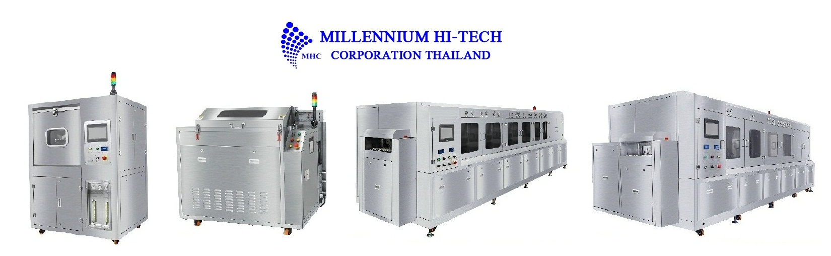
FLUX COATERS
|
BTU’s flux coating systems, the SCS608 and SCS812, handle wafers from cassettes or Front Opening Unified Pods, coats them uniformly with flux, and loads them directly onto an in-line reflow oven. To reduce cost and footprint, the flux coaters are designed with special emphasis on process control and configured with an integrated robot wafer handler. A flux coating system combined with a unloading system completes the wafer bump reflow process. Sourcing all components from a single vendor eliminates many of the integration hassles previously experienced.
|
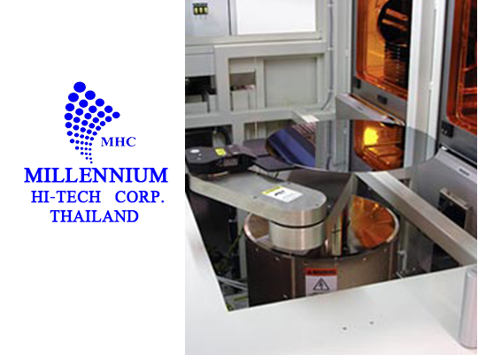
WAFER HANDLERS
|
BTU offers a variety of wafer handling systems covering wafer sizes from 100 to 300mm. These systems can be used for both loading and unloading wafers in a flux-free wafer bump reflow application. When a flux wafer bump reflow process is employed the wafer handlers can be used for unloading down stream of a BTU flux coater and reflow oven. The MHS812, a bridge tool for 200 and 300mm wafers, features a 3-axis robot and FOUP load port(s).
|
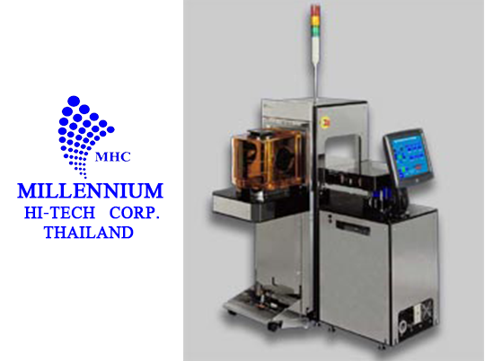
WAFER HANDLERS MHS 812
|
The MHS 812, an inline wafer handling system for 200 and 300mm wafers can be integrated with any reflow oven or cleaner. The system is typically used downstream of a flux coating system and a reflow oven. When your application calls for flux free processing, a BTU hydrogen atmosphere conveyor furnace can be paired with the MHS812 for loading and unloading. The system is FOUP compatible and both wafer sizes can be run without any hardware changes. Passive centering of the wafer reduces wafer damage during handling.
|